| CPC H01Q 1/2283 (2013.01) [H01L 21/768 (2013.01); H01L 23/3107 (2013.01); H01L 23/3128 (2013.01); H01L 23/481 (2013.01); H01L 23/528 (2013.01); H01L 23/66 (2013.01); H01L 24/14 (2013.01); H01L 24/82 (2013.01); H01Q 1/38 (2013.01); H01Q 9/04 (2013.01); H01Q 21/065 (2013.01); H01L 21/568 (2013.01); H01L 2223/6627 (2013.01); H01L 2223/6677 (2013.01); H01L 2224/13024 (2013.01); H01L 2224/13111 (2013.01); H01L 2224/13113 (2013.01); H01L 2224/13116 (2013.01); H01L 2224/13139 (2013.01); H01L 2224/13147 (2013.01); H01L 2224/13155 (2013.01); H01L 2224/18 (2013.01); H01L 2924/1431 (2013.01)] | 20 Claims |
|
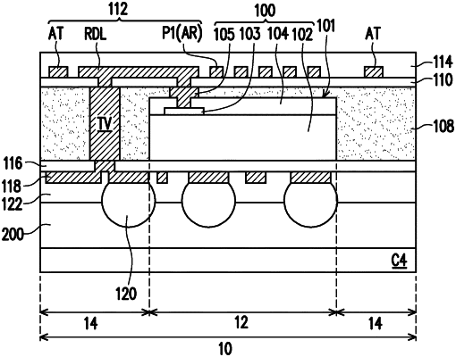
1. A semiconductor package, comprising:
a semiconductor chip having a first side and a second side opposite to each other;
an encapsulant disposed around the semiconductor chip;
a first conductive feature disposed on the first side of the semiconductor chip;
a passivation layer extending over the first conductive feature and comprising an opening exposing a portion of the first conductive feature;
a first portion of a polymer layer extending over the encapsulant and the semiconductor chip;
a first redistribution layer structure disposed at the first side of the semiconductor chip, electrically connected to the first conductive feature and extending over the first portion of the polymer layer, and
a second redistribution layer structure disposed at the second side of the semiconductor chip, wherein a semiconductor substrate of the semiconductor chip is in contact with a polymer material of the second redistribution layer structure.
|