| CPC H01L 31/1129 (2013.01) [H01L 27/14679 (2013.01); H01L 29/66893 (2013.01); H01L 29/808 (2013.01); H01L 31/112 (2013.01); H01L 31/1804 (2013.01); H01L 31/1864 (2013.01); H01L 29/1066 (2013.01)] | 20 Claims |
|
1. A method for forming a photosensitive device, the method comprising:
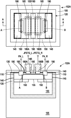
forming a sensor cavity in a silicon substrate;
forming a doped silicon layer and a germanium layer in the sensor cavity, wherein the doped silicon layer is disposed between the silicon substrate and the germanium layer;
forming a first doped region, a second doped region, a third doped region, and a fourth doped region in the germanium layer, wherein the first doped region is between the second doped region and the third doped region, the fourth doped region is over the first doped region, the first doped region includes a first type dopant, and the second doped region, the third doped region, and the fourth doped region include a second type dopant;
forming a gate over the germanium layer, wherein the gate is over the fourth doped region and the gate includes the second type dopant; and
forming a fifth doped region, a sixth doped region, and a seventh doped region in the germanium layer, wherein the fifth doped region overlaps the first doped region and the second doped region, the sixth doped region overlaps the first doped region and the third doped region, the fourth doped region is between the fifth doped region and the sixth doped region, the seventh doped region is under the gate, the fifth doped region and the sixth doped region include the first type dopant, and the seventh doped region includes the second type dopant.
|