| CPC H01L 31/1121 (2013.01) [H01L 31/0256 (2013.01); H01L 31/022408 (2013.01)] | 18 Claims |
|
1. A sensor, comprising:
a semiconductor substrate;
a first electrode and a second electrode; and
a photo-active layer between the first electrode and the second electrode, the photo-active layer including a light absorbing semiconductor,
wherein the photo-active layer has a first surface that is proximate to the first electrode, and a second surface that is proximate to the second electrode, the second surface facing the first surface such that the first surface and the second surface are opposite surfaces of the photo-active layer,
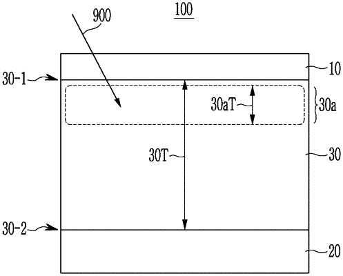
wherein the photo-active layer has a charge carrier trapping site configured to capture photo-generated charge carriers generated based on the light absorbing semiconductor absorbing incident light, and
wherein the charge carrier trapping site is at least partially defined by the first surface of the photo-active layer and in a limited portion of the photo-active layer such that a thickness of the charge carrier trapping site, extending from the first surface of the photo-active layer in a direction extending perpendicular to the first surface of the photo-active layer, is less than about 50% of a total thickness of the photo-active layer from the first surface of the photo-active layer to the second surface of the photo-active layer,
wherein the semiconductor substrate includes a charge storage electrically connected to the second electrode.
|