| CPC H01L 31/02363 (2013.01) [H01L 21/02019 (2013.01); H01L 31/068 (2013.01); H01L 31/1804 (2013.01); Y02E 10/50 (2013.01)] | 20 Claims |
|
1. A method of manufacturing a solar cell, the method comprising:
obtaining a semiconductor substrate having a first surface and a second surface opposite to the first surface;
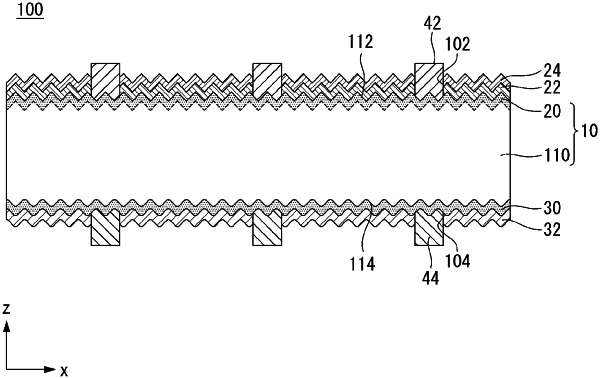
forming a first uneven member on the first surface of the semiconductor substrate, the first uneven member having a pointed pyramidal shape;
forming a second uneven member on the second surface of the semiconductor substrate, the second uneven member having a pointed pyramidal shape;
removing portions of the second uneven member on the second surface of the semiconductor substrate to form a rounded uneven member having a rounded end portion, wherein the first uneven member having a pointed pyramidal shape on the first surface of the semiconductor substrate is preserved while forming the rounded uneven member having a rounded end portion;
forming a first conductive region at the first surface of the semiconductor substrate such that the first conductive region is arranged over the first uneven member having a pointed pyramidal shape;
forming a second conductive region on the second surface of the semiconductor substrate, wherein the second conductive region comprises a semiconductor layer different from the semiconductor substrate, and wherein the second conductive region is arranged over the rounded uneven member having a rounded end portion;
forming a first electrode electrically connected to the first conductive region; and
forming a second electrode electrically connected to the second conductive region.
|