US 11,855,227 B2
Solid-state image pickup unit and electronic apparatus
Tetsuji Yamaguchi, Kanagawa (JP)
Assigned to Sony Semiconductor Solutions Corporation, Kanagawa (JP)
Filed by SONY SEMICONDUCTOR SOLUTIONS CORPORATION, Kanagawa (JP)
Filed on May 18, 2022, as Appl. No. 17/747,268.
Application 17/747,268 is a continuation of application No. 17/068,807, filed on Oct. 12, 2020, granted, now 11,367,794.
Application 17/068,807 is a continuation of application No. 16/056,139, filed on Aug. 6, 2018, granted, now 10,833,110, issued on Nov. 10, 2020.
Application 16/056,139 is a continuation of application No. 15/581,317, filed on Apr. 28, 2017, granted, now 10,074,697, issued on Sep. 11, 2018.
Application 15/581,317 is a continuation of application No. 15/581,128, filed on Apr. 28, 2017, granted, now 10,008,524, issued on Jun. 26, 2018.
Application 15/581,128 is a continuation of application No. 14/759,734, granted, now 9,954,018, issued on Apr. 24, 2018, previously published as PCT/JP2013/084053, filed on Dec. 19, 2013.
Claims priority of application No. 2013-005274 (JP), filed on Jan. 16, 2013.
Prior Publication US 2022/0278237 A1, Sep. 1, 2022
Int. Cl. H01L 29/786 (2006.01); H01L 27/146 (2006.01); H01L 29/24 (2006.01); H01L 29/16 (2006.01); H04N 25/63 (2023.01); H04N 25/70 (2023.01); H04N 25/76 (2023.01); H04N 25/13 (2023.01); H10K 19/20 (2023.01); H10K 39/32 (2023.01)
CPC H01L 29/7869 (2013.01) [H01L 27/14603 (2013.01); H01L 27/14609 (2013.01); H01L 27/14612 (2013.01); H01L 27/14621 (2013.01); H01L 27/14623 (2013.01); H01L 27/14636 (2013.01); H01L 27/14645 (2013.01); H01L 27/14665 (2013.01); H01L 29/16 (2013.01); H01L 29/24 (2013.01); H04N 25/134 (2023.01); H04N 25/63 (2023.01); H04N 25/70 (2023.01); H04N 25/76 (2023.01); H10K 19/20 (2023.02); H10K 39/32 (2023.02)] 17 Claims
OG exemplary drawing
 
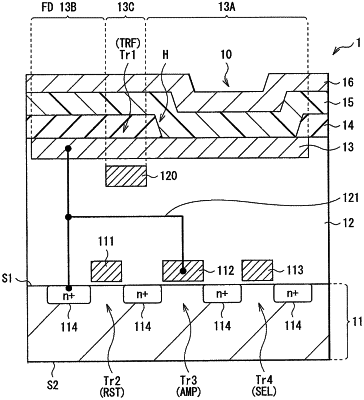
1. A light detecting device, comprising:
a photoelectric conversion layer disposed above a semiconductor substrate;
a first electrode disposed above the photoelectric conversion layer;
a second electrode disposed between the photoelectric conversion layer and the semiconductor substrate;
an oxide semiconductor layer disposed between the photoelectric conversion layer and the second electrode; and
an amplification transistor disposed at a first surface of the semiconductor substrate, a gate electrode of the amplification transistor being connected to the oxide semiconductor layer,
wherein the oxide semiconductor layer comprises a first portion configured to store electric charge generated in the photoelectric conversion layer, and
wherein the second electrode is electrically isolated from the oxide semiconductor layer and configured to transfer the electric charge stored in the first portion of the oxide semiconductor layer.