| CPC H01L 29/7851 (2013.01) [H01L 21/823431 (2013.01); H01L 21/823481 (2013.01); H01L 23/291 (2013.01); H01L 23/3171 (2013.01); H01L 27/0886 (2013.01); H01L 29/0649 (2013.01); H01L 29/1054 (2013.01); H01L 29/165 (2013.01); H01L 29/66795 (2013.01); H01L 29/66818 (2013.01); H01L 29/785 (2013.01); H01L 29/7853 (2013.01); H01L 29/7854 (2013.01); H01L 2924/0002 (2013.01)] | 20 Claims |
|
1. A method of forming a fin field effect transistor (FinFET), the method comprising:
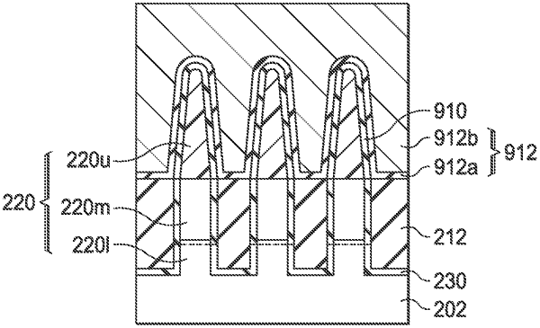
forming a first fin extending from a substrate, the first fin having one or more semiconductor layers overlying the substrate, each of the one or more semiconductor layers having a lattice constant different than a lattice constant of an underlying layer, wherein an uppermost semiconductor layer of the one or more semiconductor layers comprises a germanium-containing semiconductor material;
forming a first passivation layer over the first fin, wherein the first passivation layer over the uppermost semiconductor layer comprises an oxynitride of the germanium-containing semiconductor material;
after forming the first passivation layer, forming isolation regions along opposing sidewalls of the first fin;
removing the first passivation layer above an upper surface of the isolation regions, the first fin extending above an uppermost surface of the isolation regions and an upper surface of the first passivation layer;
etching portions of the first fin extending above the upper surface of the isolation regions to form a reshaped portion of the first fin, wherein after the etching, sidewalls of the first fin above the first passivation layer have a different slope than sidewalls of the first fin adjacent the first passivation layer;
forming a second passivation layer over the reshaped portion of the first fin, wherein the second passivation layer over the reshaped portion of the first fin comprises an oxynitride of the germanium-containing semiconductor material; and
forming a gate structure over the second passivation layer.
|