| CPC H01L 29/7848 (2013.01) [H01L 21/76243 (2013.01); H01L 29/0638 (2013.01); H01L 29/263 (2013.01)] | 9 Claims |
|
1. A method for fabricating a FDSOI device, comprising at least following steps:
step 1: providing a silicon substrate, disposing a buried oxide layer on the silicon substrate, and disposing a silicon-on-insulator (SOI) layer on the buried oxide layer;
step 2: forming a silicon-germanium (SiGe) layer on the SOI layer by means of epitaxial deposition;
step 3: oxidizing the SiGe layer by means of high-temperature oxidation, wherein germanium atoms in the SiGe layer diffuse into the SOI layer to form a SiGe channel layer, wherein a thickness of the SiGe channel layer is in a range of 60-100 A, wherein a SiO2 layer is formed on the SiGe channel layer;
step 4: removing the SiO2 layer;
step 5: passivating an upper surface of the SiGe channel layer to form a nitrogen passivation layer;
step 6: sequentially depositing a gate oxide layer, a high-k dielectric layer, and a first TiN layer on the nitrogen passivation layer;
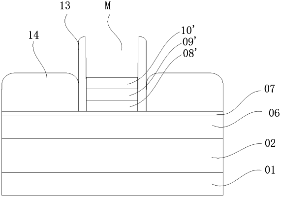
step 7: forming an amorphous silicon layer on the first TiN layer, depositing a hard mask layer on the amorphous silicon layer, then defining a gate morphology by means of a photolithography process, followed by etching sequentially the hard mask layer, the amorphous silicon layer, the first TiN layer, the high-k dielectric layer, and the gate oxide layer, to form a first stack structure;
wherein the first stack structure comprises a gate oxide layer structure, a high-k dielectric layer structure, and a first TiN layer structure that are sequentially stacked from bottom to top;
wherein step 7 further comprises: forming an amorphous silicon layer structure located on the first stack structure and forming a hard mask layer structure located on the amorphous silicon layer structure, then forming sidewalls of inner spacers, and forming an outer hard mask on sides of the first stack layer and the amorphous silicon layer structure;
step 8: growing epitaxially a raised SiGe layer at both sides of the amorphous silicon layer structure, and forming a source region and a drain region in the raised SiGe layer;
step 9: removing the hard mask layer structure and the amorphous silicon layer structure, and forming a groove between the sidewalls of the inner spacers of the first stack layer;
step 10: sequentially depositing a TaN layer, a second TiN layer, a TiAl layer, and an aluminum layer in the groove, so to form a second stack structure in the groove, wherein the first stack structure, the second stack structure and the sidewalls of the inner spacers of the first stack layer form a metal gate, wherein the sidewalls cover sides of the first stack structure and extend up to a portion of the second stack structure; and
step 11: planarizing the aluminum layer, and then forming metal interconnection.
|