| CPC H01L 29/7848 (2013.01) [H01L 29/1033 (2013.01)] | 20 Claims |
|
1. A semiconductor device, comprising:
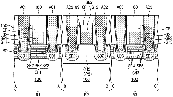
a substrate that includes a first region, a second region, and a third region;
a first channel structure on the first region, the first channel structure including a plurality of first channel patterns that are vertically stacked on the substrate;
a second channel structure on the second region, the second channel structure including a second channel pattern on the substrate;
a third channel structure on the third region, the third channel structure including a plurality of third channel patterns and a plurality of fourth channel patterns that are vertically and alternately stacked on the substrate;
a first gate electrode on the first channel structure, a second gate electrode on the second channel structure, and a third gate electrode on the third channel structure; and
a first source/drain pattern on opposite sides of the first channel structure, a second source/drain pattern on opposite sides of the second channel structure, and a third source/drain pattern on opposite sides of the third channel structure,
wherein:
the plurality of first channel patterns, the second channel pattern, and the plurality of fourth channel patterns each include a first semiconductor material, and
the plurality of third channel patterns include a second semiconductor material different from the first semiconductor material.
|