US 11,855,196 B2
Transistor with wrap-around extrinsic base
Xinshu Cai, Singapore (SG); Shyue Seng Tan, Singapore (SG); Vibhor Jain, Williston, VT (US); John J. Pekarik, Underhill, VT (US); Kien Seen Daniel Chong, Singapore (SG); Yung Fu Chong, Singapore (SG); Judson R. Holt, Ballston Lake, NY (US); Qizhi Liu, Lexington, MA (US); and Kenneth J. Stein, Sandy Hook, CT (US)
Assigned to GLOBALFOUNDRIES SINGAPORE PTE. LTD., Singapore (SG)
Filed by GLOBALFOUNDRIES Singapore Pte. Ltd., Singapore (SG)
Filed on Oct. 25, 2021, as Appl. No. 17/509,611.
Prior Publication US 2023/0129914 A1, Apr. 27, 2023
Int. Cl. H01L 29/737 (2006.01); H01L 29/66 (2006.01); H01L 29/45 (2006.01); H01L 29/10 (2006.01)
CPC H01L 29/7371 (2013.01) [H01L 29/1004 (2013.01); H01L 29/45 (2013.01); H01L 29/66242 (2013.01)] 20 Claims
OG exemplary drawing
 
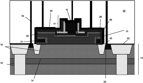
1. A structure comprising:
a substrate;
a collector region within the substrate;
an emitter region over the substrate and which comprises silicon based material;
an intrinsic base;
an extrinsic base overlapping the emitter region and the intrinsic base; and
an inverted “T” shaped spacer comprising insulator material which separates the emitter region from the extrinsic base.