| CPC H01L 29/7371 (2013.01) [H01L 29/1004 (2013.01); H01L 29/45 (2013.01); H01L 29/66242 (2013.01)] | 17 Claims |
|
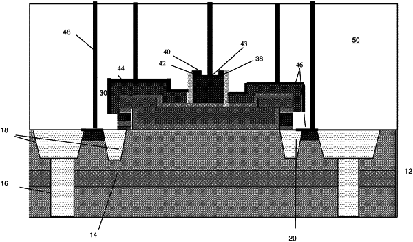
1. A structure comprising:
a substrate;
a collector region within the substrate;
an emitter region over the substrate and which entirely comprises mono-crystalline silicon based material with an insulator material thereon;
an intrinsic base under the emitter region and comprising semiconductor material;
an extrinsic base surrounding the emitter and over the intrinsic base;
a spacer separating the emitter region from the extrinsic base; and
a plurality of semiconductor materials comprising SiGe material sandwiched between undoped semiconductor material, the SiGe material comprising a raised SiGe intrinsic base, and the undoped semiconductor material comprising an intrinsic emitter region and an intrinsic collector region.
|