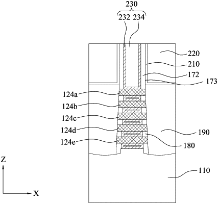
| CPC H01L 29/6681 (2013.01) [H01L 21/823431 (2013.01); H01L 29/785 (2013.01); H01L 2029/7858 (2013.01)] | 20 Claims |

|
1. A method comprising:
forming a fin structure comprising a plurality of first semiconductor layers and a plurality of second semiconductor layers alternately stacked over a substrate;
forming a dummy gate structure across the fin structure such that the dummy gate structure covers a first portion of the fin structure while second portions of the fin structure are exposed;
removing the exposed second portions of the fin structure;
after removing the exposed second portions of the fin structure, performing a first oxygen-removal process, using hydrogen radicals, to remove oxv ens in the first semiconductor layers;
after removing the exposed second portions of the fin structure, performing a second oxygen-removal process, using a hydrogen-containing gas mixture, to remove a native oxide layer formed on sidewalls of the first semiconductor layers, wherein the hydrogen radicals used in the first oxygen-removal process has sizes smaller than the hydrogen-containing gas mixture used in the second oxygen-removal process;
after performing the first oxygen-removal process, performing a selective etching process, using an etching gas mixture comprising a hydrogen-containing gas and an F2 gas, to laterally recess the first semiconductor layers in the first portion of the fin structure, wherein the selective etching process etches the first semiconductor layers at a faster etching rate than etching the second semiconductor layers;
forming inner spacers on opposite end surfaces of the laterally recessed first semiconductor layers of the first portion of the fin structure;
forming source/drain epitaxial structures on opposite end surfaces of the second semiconductor layers in the first portion of the fin structure;
removing the dummy gate structure to expose the first portion of the fin structure;
removing the laterally recessed first semiconductor layers in the exposed first portion of the fin structure while leaving the second semiconductor layers in the exposed first portion of the fin structure suspended above the substrate; and
forming a gate structure to surround each of the suspended second semiconductor layers.
|