| CPC H01L 29/66795 (2013.01) [H01L 21/20 (2013.01); H01L 21/823431 (2013.01); H01L 27/0924 (2013.01); H01L 29/41791 (2013.01); H01L 29/785 (2013.01)] | 20 Claims |
|
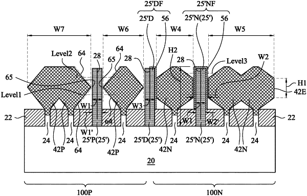
1. A method comprising:
forming a first semiconductor fin and a first dielectric fin in an n-type Fin Field-Effect (FinFET) region;
forming a second semiconductor fin and a second dielectric fin in a p-type FinFET region;
forming a first epitaxy mask to cover the second semiconductor fin and the second dielectric fin;
performing a first epitaxy process to form an n-type epitaxy region based on the first semiconductor fin;
removing the first epitaxy mask, wherein when the removing the first epitaxy mask is stopped, a remaining portion of the first epitaxy mask remains on the second dielectric fin;
forming a second epitaxy mask to cover the n-type epitaxy region and the first dielectric fin;
performing a second epitaxy process to form a p-type epitaxy region based on the second semiconductor fin; and
removing the second epitaxy mask and the remaining portion of the first epitaxy mask.
|