| CPC H01L 29/66545 (2013.01) [H01L 21/02178 (2013.01); H01L 21/02181 (2013.01); H01L 21/56 (2013.01); H01L 21/82 (2013.01); H01L 23/28 (2013.01); H01L 29/66795 (2013.01); H01L 29/785 (2013.01)] | 20 Claims |
|
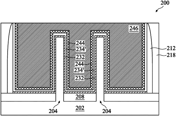
1. A semiconductor structure, comprising:
an interfacial layer disposed over a semiconductor fin;
a high-k gate dielectric layer disposed over the interfacial layer, wherein the high-k gate dielectric layer includes a first metal;
a metal oxide layer disposed between the high-k gate dielectric layer and the interfacial layer, wherein the metal oxide layer is configured to form a dipole moment with the interfacial layer, wherein the metal oxide layer includes a second metal different from the first metal, and wherein concentration of the second metal gradually decreases within the metal oxide layer; and
a metal gate electrode disposed over the high-k gate dielectric layer.
|
|
8. A semiconductor structure, comprising:
a semiconductor fin disposed over a substrate;
an interfacial layer disposed over a channel region of the semiconductor fin;
an oxide layer disposed over the interfacial layer, the oxide layer including a first metal oxide, wherein concentration of a metal in the first metal oxide is graded within the oxide layer;
a gate dielectric layer disposed over the oxide layer, the gate dielectric layer including a second metal oxide that is different from the first metal oxide;
a metal halide layer disposed over the gate dielectric layer; and
a metal gate electrode disposed over the metal halide layer.
|
|
15. A semiconductor structure, comprising:
a semiconductor fin protruding from a substrate;
an interfacial layer disposed over the semiconductor fin, the interfacial layer including a first oxide;
a high-k gate dielectric layer disposed over the interfacial layer, wherein the high-k gate dielectric layer includes a second oxide, and wherein the second oxide includes a first metal;
a first metal-containing layer disposed between and directly contacting the interfacial layer and the high-k gate dielectric layer, wherein the first metal-containing layer includes a second metal that differs from the first metal, and wherein concentration of the second metal gradually decreases from bottom surface of the high-k gate dielectric layer toward a top surface of the interfacial layer;
a second metal-containing layer disposed over the high-k gate dielectric layer; and
a metal gate electrode disposed over the second metal-containing layer.
|