US 11,855,172 B2
Semiconductor device and method for fabricating the same
Beom-Yong Kim, Gyeonggi-do (KR)
Assigned to SK hynix Inc., Gyeonggi-do (KR)
Filed by SK hynix Inc., Gyeonggi-do (KR)
Filed on May 10, 2022, as Appl. No. 17/741,204.
Application 17/741,204 is a continuation of application No. 16/780,637, filed on Feb. 3, 2020, granted, now 11,342,437.
Application 16/780,637 is a continuation of application No. 16/233,582, filed on Dec. 27, 2018, granted, now 10,593,777, issued on Mar. 17, 2020.
Claims priority of application No. 10-2018-0081861 (KR), filed on Jul. 13, 2018.
Prior Publication US 2022/0271143 A1, Aug. 25, 2022
This patent is subject to a terminal disclaimer.
Int. Cl. H01L 29/51 (2006.01); H01L 29/49 (2006.01); H01L 29/06 (2006.01); H01L 29/94 (2006.01); H01L 21/28 (2006.01); H01L 49/02 (2006.01); H10B 12/00 (2023.01)
CPC H01L 29/517 (2013.01) [H01L 21/28088 (2013.01); H01L 28/60 (2013.01); H01L 29/0607 (2013.01); H01L 29/4966 (2013.01); H01L 29/94 (2013.01); H10B 12/30 (2023.02)] 10 Claims
OG exemplary drawing
 
1. A capacitor comprising:
a bottom electrode;
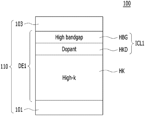
a dielectric layer formed on the bottom electrode, and including an intermixed compound in which two or more high-k materials are mixed;
a top electrode formed on the dielectric layer; and
an interface control layer formed between the dielectric layer and the top electrode, and including a reduction preventing material and a high work function material that is sequentially stacked one on the other,
wherein the reduction preventing material is formed between the dielectric layer and the top electrode, and
wherein the high work function material is formed between the reduction preventing material and the top electrode.