| CPC H01L 29/4991 (2013.01) [H01L 21/28141 (2013.01); H01L 21/31116 (2013.01); H01L 29/41775 (2013.01); H01L 29/6653 (2013.01); H01L 29/6656 (2013.01); H10B 10/00 (2023.02); H10B 12/00 (2023.02)] | 20 Claims |
|
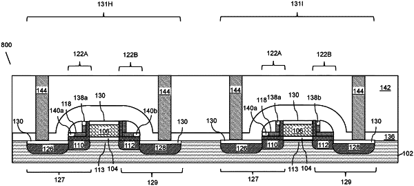
1. A metal oxide semiconductor field effect transistor (MOSFET), comprising:
a substrate comprising a source region and drain region;
a channel region between the source region and drain region;
a gate dielectric layer on a surface of the substrate and over the channel region;
a gate on the gate dielectric layer;
a first sidewall spacer on a first sidewall of the gate, comprising:
a first oxide layer including a first portion extending along the first sidewall of the gate and a second portion extending along the surface of the substrate; and
a nitride layer on the first oxide layer, and including a first air gap having an end that is substantially aligned with an end of the first portion of the first oxide layer, and a second air gap having an end that is substantially aligned with an end of the second portion of the first oxide layer; and
an etch stop layer on the first sidewall spacer, wherein the etch stop layer defines the end of the first air gap and the end of the second air gap.
|