| CPC H01L 29/42356 (2013.01) [H01L 23/5286 (2013.01); H01L 27/092 (2013.01); H01L 29/41775 (2013.01); H01L 29/42376 (2013.01)] | 19 Claims |
|
1. A semiconductor device comprising:
a substrate including a first region and a second region, wherein the first and second regions are spaced apart from each other with a device isolation layer interposed therebetween;
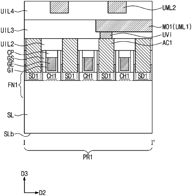
a first gate electrode and a second gate electrode on a first surface of the substrate, wherein the first and second gate electrodes are respectively on the first region and the second region, extend in a first direction, and are aligned with each other in the first direction;
an insulating separation pattern separating the first gate electrode and the second gate electrode from each other and extending in a second direction that traverses the first direction;
a connection structure electrically connecting the first gate electrode to the second gate electrode; and
a conductive line on a second surface of the substrate, wherein the second surface of the substrate is opposite the first surface of the substrate,
wherein the conductive line extends in the second direction and vertically overlaps the insulating separation pattern,
wherein the first gate electrode is on a first active pattern, and the first active pattern includes first channel regions that are vertically stacked, and
wherein the second gate electrode is on a second active pattern, and the second active pattern includes second channel regions that are vertically stacked.
|