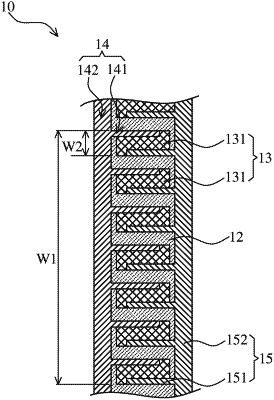
| CPC H01L 29/41733 (2013.01) [G02F 1/1368 (2013.01); G02F 1/13454 (2013.01); G09G 3/3674 (2013.01); H01L 27/1218 (2013.01); G02F 1/133305 (2013.01); G02F 1/133345 (2013.01); G09G 2300/0408 (2013.01)] | 20 Claims |

|
1. A thin film transistor structure, comprising:
a gate layer comprising a plurality of gate patterns;
a gate insulating layer covering the gate layer;
an active layer disposed on the gate insulating layer, wherein the active layer comprises a plurality of active patterns, and positions of the plurality of active patterns are respectively aligned with positions of the plurality of gate patterns;
a comb-shaped source disposed on the active layer and comprising a plurality of source comb tooth portions and a source comb handle portion, wherein the plurality of source comb tooth portions are connected to the source comb handle portion; and
a comb-shaped drain disposed on the active layer and comprising a plurality of drain comb tooth portions and a drain comb handle portion, wherein the plurality of drain comb tooth portions are connected to the drain comb handle portion, wherein the plurality of source comb tooth portions and the plurality of drain comb tooth portions are arranged alternately on the active layer in a direction, and the plurality of active patterns are each provided with a corresponding one of the plurality of source comb tooth portions and a corresponding one of the plurality of drain comb tooth portions;
wherein each of the plurality of active patterns is located only between one of two adjacent of the plurality of source comb tooth portions and one of the plurality of drain comb tooth portions located between the two adjacent of the plurality of source comb tooth portions, and there is no active pattern between the other one of the two adjacent of the plurality of source comb tooth portions and the one of the plurality of drain comb tooth portions located between the two adjacent of the plurality of source comb tooth portions.
|