| CPC H01L 29/407 (2013.01) [H01L 29/0623 (2013.01); H01L 29/1095 (2013.01); H01L 29/404 (2013.01); H01L 29/7397 (2013.01)] | 11 Claims |
|
1. A semiconductor device, comprising:
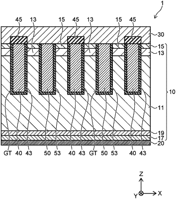
a semiconductor part including a first semiconductor layer of a first conductivity type and a second semiconductor layer of a second conductivity type, the semiconductor part including an active region and a termination region, the termination region being provided around the active region, the first semiconductor layers being provided in the active region and extending into the termination region, the second semiconductor layer being provided in the active region;
a first electrode provided at a back surface of the semiconductor part, the first electrode being provided on the active region and the termination region;
a second electrode provided at a front surface of the semiconductor part, the second electrode being provided on the active region, the second semiconductor layer being provided between the first semiconductor layer and the second electrode;
a plurality of third electrodes provided between the first electrode and the second electrode, the plurality of third electrodes each extending into the first semiconductor layer through the second semiconductor layer, the plurality of third electrodes each being electrically insulated from the semiconductor part by a first insulating film and being electrically insulated from the second electrode by a second insulating film; and
a plurality of fourth electrodes provided between the first electrode and the second electrode, the plurality of fourth electrodes each extending into the first semiconductor layer through the second semiconductor layer, the plurality of fourth electrodes each being isolated from the semiconductor part by a third insulating film, the plurality of fourth electrodes each including a material of a larger thermal conductivity than a thermal conductivity of a material of each of the third electrodes,
the plurality of fourth electrodes being arranged along the front surface of the semiconductor part, the plurality of third electrodes each being provided between two fourth electrodes of the plurality of fourth electrodes, the two fourth electrodes being arranged next to each other, the plurality of fourth electrodes including a fourth electrode located at an end of the plurality of third and fourth electrodes arranged along the front surface of the semiconductor part,
the semiconductor part including a sixth semiconductor layer of the second conductivity type, the sixth semiconductor layer being provided on the first semiconductor layer at the front surface side of the semiconductor part, the sixth semiconductor layer surrounding the active region along a boundary between the active region and the termination region,
the fourth electrode located at the end of the third and fourth electrodes is proximate to the sixth semiconductor layer,
the device further comprising a fifth electrode extending into the sixth semiconductor layer from the front surface side of the semiconductor part, the fifth electrode being electrically insulated from the semiconductor part by a fourth insulating film, and
the fifth electrode including a material having a larger thermal conductivity than the thermal conductivity of the material of the third electrode, the fifth electrode extending into the first semiconductor layer through the sixth semiconductor layer.
|