| CPC H01L 29/401 (2013.01) [H01L 21/283 (2013.01); H01L 21/28518 (2013.01); H01L 21/76802 (2013.01); H01L 21/76831 (2013.01); H01L 21/76877 (2013.01); H01L 29/456 (2013.01); H01L 29/665 (2013.01)] | 20 Claims |
|
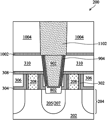
1. A semiconductor device, comprising:
a source/drain region adjacent a gate structure on a semiconductor substrate;
an insulating layer formed over the semiconductor substrate and having an interface with a top surface of the source/drain region;
a contact element extending through the insulating layer to the source/drain region, wherein the contact element includes:
a silicide region having a substantially U-shape in cross-section, wherein the silicide region extends above the interface;
a liner layer disposed along a sidewall of a metal contact layer and interfacing a top surface of the U-shaped silicide region, the liner layer having a sidewall collinear with a sidewall of the U-shaped silicide region; and
the metal contact layer over the U-shaped silicide region and within the U-shape.
|