US 11,855,152 B2
Ultrawide bandgap semiconductor devices including magnesium germanium oxides
Petar Atanackovic, Henley Beach South (AU)
Assigned to Silanna UV Technologies Pte Ltd, Singapore (SG)
Filed by Silanna UV Technologies Pte Ltd, Singapore (SG)
Filed on Feb. 18, 2022, as Appl. No. 17/651,711.
Application 17/651,711 is a continuation of application No. PCT/IB2021/060414, filed on Nov. 10, 2021.
Prior Publication US 2023/0146938 A1, May 11, 2023
This patent is subject to a terminal disclaimer.
Int. Cl. H01L 33/26 (2010.01); H01L 29/24 (2006.01); H01L 31/032 (2006.01); H01L 21/02 (2006.01); C30B 29/32 (2006.01); H01L 21/225 (2006.01); H01L 33/00 (2010.01)
CPC H01L 29/24 (2013.01) [C30B 29/32 (2013.01); H01L 21/02565 (2013.01); H01L 21/02576 (2013.01); H01L 21/02579 (2013.01); H01L 21/02631 (2013.01); H01L 21/2252 (2013.01); H01L 31/032 (2013.01); H01L 33/0029 (2013.01); H01L 33/26 (2013.01)] 31 Claims
OG exemplary drawing
 
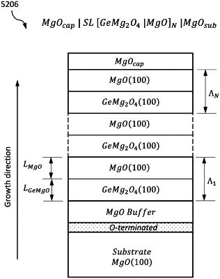
1. A semiconductor structure comprising:
a substrate comprising a substantially single crystal substrate material; and
an epitaxial layer of MgxGe1-xO2-x on the substrate, with x having a value of 0≤x<1;
wherein the epitaxial layer of MgxGe1-xO2-x has a crystal symmetry compatible with the substrate material.