| CPC H01L 29/1045 (2013.01) [H01L 29/0646 (2013.01); H01L 29/1054 (2013.01); H01L 29/165 (2013.01); H01L 29/205 (2013.01); H01L 29/40111 (2019.08); H01L 29/40114 (2019.08); H01L 29/42324 (2013.01); H01L 29/4983 (2013.01); H01L 29/516 (2013.01); H01L 29/66431 (2013.01); H01L 29/66659 (2013.01); H01L 29/66977 (2013.01); H01L 29/685 (2013.01); H01L 29/785 (2013.01); H01L 29/7881 (2013.01); H01L 29/802 (2013.01); H10B 12/30 (2023.02); H10B 41/30 (2023.02); H10B 51/30 (2023.02); H10B 63/00 (2023.02); H01L 29/6684 (2013.01); H01L 29/66825 (2013.01); H01L 29/788 (2013.01); H01L 29/78391 (2014.09)] | 7 Claims |
|
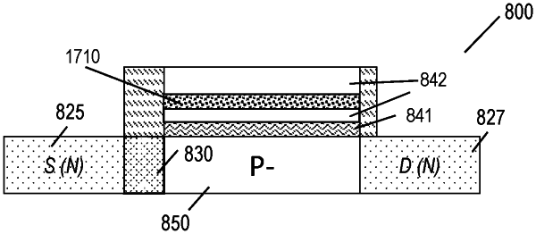
1. A semiconductor device comprising:
a source terminal;
a drain terminal, wherein the source terminal and the drain terminal are formed on either sides of a channel region designated on a substrate;
an energy barrier adjacent to the source terminal and the channel region; and
a conductive gate stack formed over the channel region, wherein the conductive gate stack comprises a first gate dielectric layer on the channel region, a metal layer on an upper surface of the first gate dielectric layer, a layer of a ferroelectric material on an upper surface of the metal layer, and an electrically conductive material layer on an upper surface of the layer of the ferroelectric material.
|
|
4. A semiconductor device comprising:
a semiconductor fin formed on a substrate, the semiconductor fin comprising:
a source terminal that is doped using a first dopant;
a drain terminal that is doped using a second dopant at a first concentration; and
a channel that is doped using the second dopant at a second concentration, wherein the second concentration is lower than the first concentration,
a gate stack formed over the channel, wherein the gate stack comprises first gate dielectric layer on the channel, a metal layer on an upper surface of the first gate dielectric layer, a layer of a ferroelectric material on an upper surface of the metal layer, and an electrically conductive material layer on an upper surface of the layer of a ferroelectric material; and
a first energy barrier adjacent to the source terminal and the channel region, and a second energy barrier adjacent to the drain terminal and the channel region.
|
|
7. A semiconductor device comprising:
a semiconductor fin formed on a substrate, the semiconductor fin comprising:
a source terminal that is doped using a first dopant;
a drain terminal that is doped using a second dopant at a first concentration; and
a channel that is doped using the second dopant at a second concentration,
wherein the second concentration is lower than the first concentration; and
a gate stack formed over the channel,
wherein the gate stack comprises:
a first gate dielectric layer on the channel, a metal layer on an upper surface of the first gate dielectric layer, a layer of a ferroelectric material on an upper surface of the metal layer, and an electrically conductive material layer on an upper surface of the layer of a ferroelectric material; and
a second gate dielectric layer on an upper surface of the layer of a ferroelectric material,
wherein the layer of a ferroelectric material is interposed between the first dielectric layer and the second dielectric layer.
|