| CPC H01L 29/0852 (2013.01) [H01L 29/1608 (2013.01); H01L 29/41741 (2013.01); H01L 29/4236 (2013.01); H01L 29/66068 (2013.01); H01L 29/7806 (2013.01); H01L 29/7813 (2013.01); H01L 21/049 (2013.01); H01L 21/0465 (2013.01); H01L 21/0485 (2013.01); H01L 21/0495 (2013.01)] | 20 Claims |

|
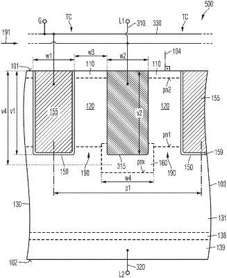
1. A method for producing a semiconductor component, the method comprising:
forming a silicon carbide substrate comprising a body layer formed on a section of a main layer, and a source layer formed on a section of the body layer, a conductivity type of the body layer being opposite to a conductivity type of the source layer and of a drift layer in the main layer;
forming gate trenches and contact trenches extending through the source layer and the body layer, the gate trenches and contact trenches alternating along a first horizontal direction parallel to a first main surface of the silicon carbide substrate;
forming a gate dielectric in the gate trenches;
forming a metal structure which comprises first sections adjoining the gate dielectric in the gate trenches and second sections in the contact trenches, the second sections adjoining body regions formed from sections of the body layer and source regions formed from sections of the source layer; and
removing third sections of the metal structure that connect the first sections to the second sections.
|