US 11,855,137 B2
SOI device structure for robust isolation
Lin-Chen Lu, Kaohsiung (TW); Gulbagh Singh, Tainan (TW); Tsung-Han Tsai, Miaoli County (TW); and Po-Jen Wang, Taichung (TW)
Assigned to TAIWAN SEMICONDUCTOR MANUFACTURING COMPANY, LTD.
Filed by Taiwan Semiconductor Manufacturing Company, Ltd., Hsinchu (TW)
Filed on Feb. 4, 2022, as Appl. No. 17/592,997.
Application 17/592,997 is a continuation of application No. 16/886,386, filed on May 28, 2020, granted, now 11,257,902.
Prior Publication US 2022/0157935 A1, May 19, 2022
Int. Cl. H01L 29/06 (2006.01); H01L 21/762 (2006.01); H01L 23/66 (2006.01); H01L 29/10 (2006.01)
CPC H01L 29/0649 (2013.01) [H01L 21/76254 (2013.01); H01L 23/66 (2013.01); H01L 29/1095 (2013.01)] 9 Claims
OG exemplary drawing
 
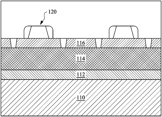
1. A method of forming a semiconductor device, comprising:
providing a first substrate;
forming a buried oxide layer over the first substrate;
forming an active layer over the buried oxide layer; and
forming a semiconductor isolation layer between the buried oxide layer and the first substrate through an ion implantation process, wherein the semiconductor isolation layer fully overlays the first substrate.