| CPC H01L 29/0623 (2013.01) [H01L 29/24 (2013.01); H01L 29/66969 (2013.01); H01L 29/7802 (2013.01); H01L 29/872 (2013.01); H02P 27/06 (2013.01)] | 21 Claims |
|
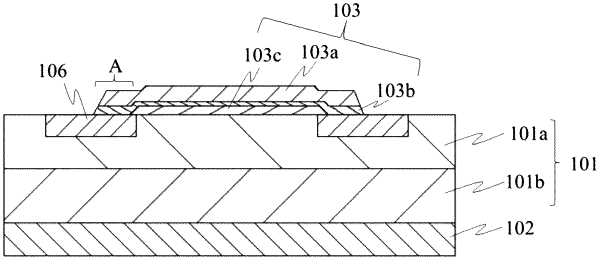
1. A semiconductor device comprising:
a semiconductor layer; and
an electrode layer provided on the semiconductor layer and including a first electrode layer and a second electrode layer provided on the first electrode layer,
wherein an outer edge portion of the second electrode layer is located outside an outer edge portion of the first electrode layer,
wherein the semiconductor layer includes an electric field relaxation region with a different electrical resistivity from the semiconductor layer, and
wherein the electric field relaxation region overlaps at least a part of a portion of the second electrode layer located outside the outer edge portion of the first electrode layer in a plan view.
|