| CPC H01L 27/156 (2013.01) [H01L 33/405 (2013.01); H01L 33/44 (2013.01); H01L 33/52 (2013.01); H01L 33/60 (2013.01)] | 5 Claims |
|
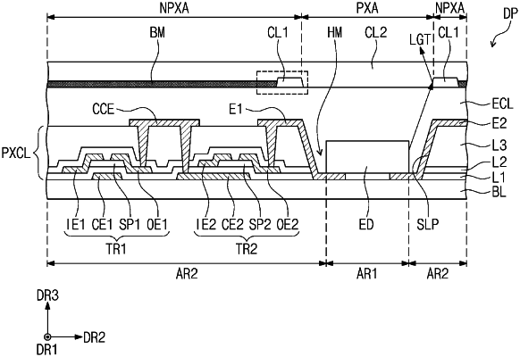
1. A display device comprising:
a base layer;
a pixel circuit layer disposed on the base layer and comprising a transistor and insulation layers, each of the insulation layers having a groove;
a first electrode electrically connected to the transistor;
a second electrode spaced apart from the first electrode and configured to receive a power source voltage;
a light emitting element electrically connected to the first electrode and the second electrode and disposed in the groove;
a first refraction layer overlapping an area adjacent to an emission area on which the light emitting element is disposed and having a first refractive index; and
a second refraction layer overlapping the emission area and having a second refractive index larger than the first refractive index.
|