| CPC H01L 27/14643 (2013.01) [H01L 27/1461 (2013.01); H01L 27/14636 (2013.01); H01L 27/14689 (2013.01)] | 3 Claims |
|
1. A semiconductor device comprising a photosensor including a photodiode formed on a substrate,
wherein the photodiode includes:
a cathode electrode;
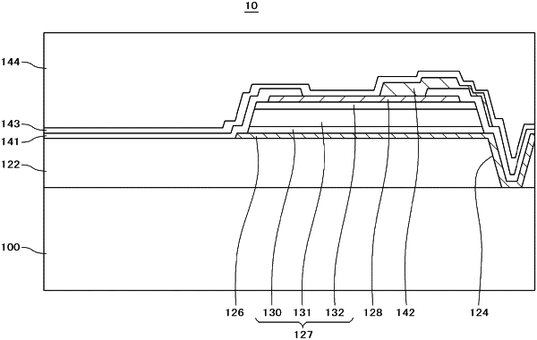
a laminated structure that is formed on the cathode electrode and in which an N+ layer, an I layer, and a P+ layer are laminated in this order;
an anode electrode formed on the P+ layer;
a first insulating film formed so as to cover a portion of the anode electrode and edges of the laminated structure; and
a metal wiring connected to the anode electrode, and
the edges of the laminated structure are formed in forward tapered shapes in a cross-sectional view,
wherein each of the N+ layer, the I layer, and the P+ layer is formed of a-Si film,
wherein the crystallinity of the P+ layer is more deteriorated in comparison with the crystallinity of the I layer, and
wherein boron ion implantation is executed on the P+ layer after the P+ layer is formed.
|