| CPC H01L 27/14636 (2013.01) [H01L 27/14603 (2013.01); H01L 27/14621 (2013.01); H01L 27/14627 (2013.01)] | 17 Claims |
|
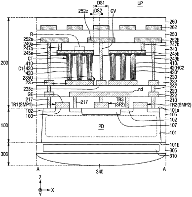
1. An image sensor comprising:
a plurality of unit pixels, each comprising:
a substrate including first and second sides which are opposite to each other;
a photoelectric conversion layer in the substrate; and
a wiring structure adjacent the first side of the substrate;
wherein the wiring structure includes:
a first capacitor;
a second capacitor spaced from the first capacitor;
a plurality of edge vias arranged along edges of the unit pixel; and
a plurality of central vias interposed between the first capacitor and the second capacitor,
wherein each of the first capacitor and the second capacitor includes a lower electrode, a capacitor dielectric film and an upper electrode which are sequentially stacked on the first side of the substrate, and
the wiring structure includes a lower electrode pad connected to the lower electrode, and an upper electrode pad connected to the upper electrode, and the lower electrode pad connects the lower electrode of the first capacitor and the lower electrode of the second capacitor.
|