| CPC H01L 27/14627 (2013.01) [H01L 27/1464 (2013.01); H01L 27/14629 (2013.01); H01L 27/1463 (2013.01); H01L 27/14621 (2013.01); H01L 27/14623 (2013.01); H01L 27/14645 (2013.01)] | 20 Claims |
|
1. A light detecting device, comprising: a plurality of pixel regions, wherein a pixel region of the plurality of pixel regions includes:
a semiconductor substrate that includes a photoelectric conversion region;
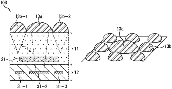
a lens array including a plurality of lenses on a first surface side of the semiconductor substrate, wherein
the plurality of lenses includes a first lens, a plurality of second lenses, and a plurality of third lenses,
the plurality of second lenses is in a first row of the lens array, the first lens is in a second row of the lens array, the plurality of third lenses is in a third row of the lens array,
in a plan view of the light detecting device, the first lens is sandwiched between the first row of the lens array and the third row of the lens array, and
a size of the first lens is larger than a size of each of the plurality of second lenses in the first row and a size of each of the plurality of third lenses in the third row;
and a wiring layer on a second surface side of the semiconductor substrate opposite to the first surface side.
|