| CPC H01L 27/1461 (2013.01) [H01L 27/14636 (2013.01); H01L 27/14643 (2013.01)] | 11 Claims |

|
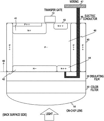
1. A solid-state imaging element, comprising:
a first photoelectric conversion element;
a first accumulation part configured to accumulate electric charges photoelectrically converted by the first photoelectric conversion element;
a second photoelectric conversion element;
a second accumulation part on a first face of a substrate and configured to accumulate electric charges photoelectrically converted by the second photoelectric conversion element; and
a connection part connected to the second accumulation part and configured to transfer the electric charges accumulated in the second accumulation part to a second face of the substrate.
|