US 11,855,107 B2
Manufacturing method for image sensor structure
Xiaoxu Kang, Shanghai (CN)
Assigned to SHANGHAI IC R&D CENTER CO., LTD., Shanghai (CN)
Filed by SHANGHAI IC R&D CENTER CO., LTD., Shanghai (CN)
Filed on Feb. 6, 2022, as Appl. No. 17/665,536.
Application 17/665,536 is a division of application No. 16/618,343, granted, now 11,276,718, previously published as PCT/CN2017/091083, filed on Jun. 30, 2017.
Claims priority of application No. 201710516396.9 (CN), filed on Jun. 29, 2017; application No. 201710516399.2 (CN), filed on Jun. 29, 2017; application No. 201710516500.4 (CN), filed on Jun. 29, 2017; and application No. 201710517118.5 (CN), filed on Jun. 29, 2017.
Prior Publication US 2022/0262833 A1, Aug. 18, 2022
Int. Cl. H01L 27/146 (2006.01)
CPC H01L 27/14605 (2013.01) [H01L 27/14683 (2013.01)] 12 Claims
OG exemplary drawing
 
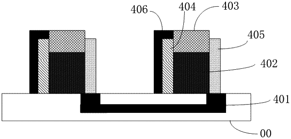
1. A manufacturing method for an image sensor structure, comprising the process of preparing an effective pixel array, wherein the preparing method of each effective pixel comprises: forming a first conductivity type sensitive material layer as a detection structure layer, and forming a second conductivity type non-sensitive material layer as a blind pixel structure layer; wherein a first end of the detection structure layer and a first end of the blind pixel structure layer are jointly connected to a first shared extraction electrode, and a second end of the detection structure layer and a second end of the blind pixel structure layer are respectively connected to a second extraction electrode and a third extraction electrode.