| CPC H01L 27/14603 (2013.01) [H01L 27/1461 (2013.01); H01L 27/14623 (2013.01); H01L 27/14685 (2013.01); H04N 25/75 (2023.01); H04N 25/77 (2023.01); H01L 27/1463 (2013.01); H01L 27/1464 (2013.01); H01L 27/14634 (2013.01); H01L 31/107 (2013.01)] | 19 Claims |
|
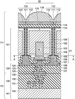
1. A solid-state imaging device comprising:
a first semiconductor substrate that includes a grid-shaped first trench provided in a first surface, and a second trench provided along a bottom of the first trench; and
a plurality of photoelectric conversion elements that is provided in the first semiconductor substrate,
wherein each of the photoelectric conversion elements includes:
a photoelectric conversion region that is provided in an element region defined by the first trench and the second trench in the first semiconductor substrate, and is configured to photoelectrically convert incident light to generate charges;
a first semiconductor region that surrounds the photoelectric conversion region in the element region;
a first contact that makes contact with the first semiconductor region at the bottom of the first trench;
a first electrode that makes contact with the first contact in the first trench;
a second semiconductor region that is provided in a region of the element region making contact with the first semiconductor region, and has a first conductivity type the same as the first semiconductor region;
a third semiconductor region that is a region making contact with the second semiconductor region in the element region, is provided between the second semiconductor region and the first surface, and has a second conductivity type opposite to that of the first conductivity type;
a second contact that is provided on the first surface so as to make contact with the third semiconductor region; and
a second electrode that makes contact with the second contact, and
a height of the first contact from the first surface is different from a height of the third semiconductor region from the first surface.
|