| CPC H01L 27/1255 (2013.01) [G09G 3/3225 (2013.01); H01L 27/124 (2013.01); H01L 27/1222 (2013.01); H10K 59/1213 (2023.02); H10K 59/1216 (2023.02); H10K 59/131 (2023.02)] | 14 Claims |
|
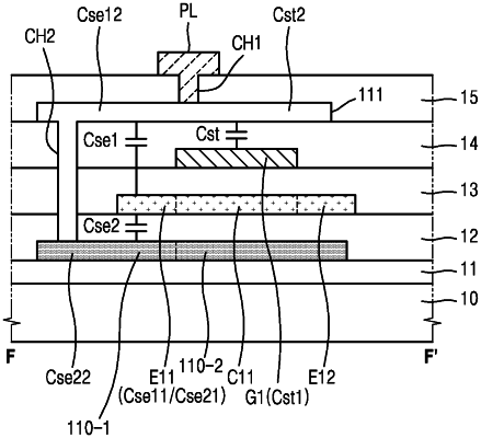
1. A display device comprising:
a bottom layer;
a semiconductor layer, wherein at least a portion of the semiconductor layer overlaps the bottom layer;
a first electrode layer disposed on the semiconductor layer and overlapping a channel region of the semiconductor layer;
a second electrode layer overlapping the first electrode layer and the semiconductor layer;
a power line disposed on the second electrode layer and electrically connected to the bottom layer and the second electrode layer; and
a light-emitting device comprising a pixel electrode, a common electrode facing the pixel electrode, and an emission layer between the pixel electrode and the common electrode,
wherein the second electrode layer is between the first electrode layer and the power line and is electrically insulated from the first electrode layer, and
wherein a first end of the semiconductor layer is electrically connected to the power line and a second end of the semiconductor layer is electrically connected to the pixel electrode.
|