US 11,855,098 B2
Semiconductor devices having dipole-inducing elements
Cheng-Yen Tsai, New Taipei (TW); Ming-Chi Huang, Zhubei (TW); Zoe Chen, Taipei (TW); Wei-Chin Lee, Taipei (TW); Cheng-Lung Hung, Hsinchu (TW); Da-Yuan Lee, Jhubei (TW); Weng Chang, Hsinchu (TW); and Ching-Hwanq Su, Tainan (TW)
Assigned to TAIWAN SEMICONDUCTOR MANUFACTURING COMPANY, LTD., Hsinchu (TW)
Filed by Taiwan Semiconductor Manufacturing Co., Ltd., Hsinchu (TW)
Filed on Nov. 14, 2022, as Appl. No. 17/986,379.
Application 17/986,379 is a continuation of application No. 17/120,921, filed on Dec. 14, 2020, granted, now 11,502,080.
Application 17/120,921 is a continuation of application No. 16/716,248, filed on Dec. 16, 2019, granted, now 10,868,013, issued on Dec. 15, 2020.
Application 16/716,248 is a continuation of application No. 16/421,759, filed on May 24, 2019, granted, now 10,510,756, issued on Dec. 17, 2019.
Application 16/421,759 is a continuation of application No. 15/998,780, filed on Aug. 15, 2018, granted, now 10,304,835, issued on May 28, 2019.
Prior Publication US 2023/0073400 A1, Mar. 9, 2023
This patent is subject to a terminal disclaimer.
Int. Cl. H01L 29/66 (2006.01); H01L 29/51 (2006.01); H01L 29/78 (2006.01); H01L 27/092 (2006.01); H01L 21/324 (2006.01); H01L 29/08 (2006.01); H01L 21/768 (2006.01); H01L 21/28 (2006.01); H01L 21/8238 (2006.01); H01L 21/02 (2006.01); H01L 29/10 (2006.01); H01L 21/321 (2006.01); H01L 21/027 (2006.01); H01L 29/49 (2006.01)
CPC H01L 27/0924 (2013.01) [H01L 21/0228 (2013.01); H01L 21/0271 (2013.01); H01L 21/02318 (2013.01); H01L 21/02321 (2013.01); H01L 21/28088 (2013.01); H01L 21/324 (2013.01); H01L 21/3212 (2013.01); H01L 21/76829 (2013.01); H01L 21/823821 (2013.01); H01L 21/823857 (2013.01); H01L 21/823864 (2013.01); H01L 21/823871 (2013.01); H01L 29/0847 (2013.01); H01L 29/1033 (2013.01); H01L 29/517 (2013.01); H01L 29/6681 (2013.01); H01L 29/66545 (2013.01); H01L 29/66553 (2013.01); H01L 29/7851 (2013.01); H01L 27/092 (2013.01); H01L 29/4966 (2013.01); H01L 29/513 (2013.01); H01L 29/7848 (2013.01)] 20 Claims
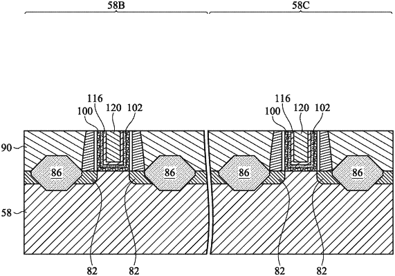
OG exemplary drawing
 
1. A device comprising:
a channel region above a substrate;
an interface layer on the channel region, the interface layer being doped with a dipole-inducing element, a first concentration of the dipole-inducing element in the interface layer increasing in a first direction extending away from the channel region;
a high-k dielectric layer on the interface layer, the high-k dielectric layer being doped with the dipole-inducing element, a second concentration of the dipole-inducing element in the high-k dielectric layer decreasing in the first direction extending away from the channel region; and
a gate electrode on the high-k dielectric layer.