| CPC H01L 27/0921 (2013.01) [H01L 21/2255 (2013.01); H01L 21/823807 (2013.01); H01L 21/823821 (2013.01); H01L 21/823878 (2013.01); H01L 21/823892 (2013.01); H01L 27/0924 (2013.01); H01L 29/0653 (2013.01); H01L 29/1054 (2013.01); H01L 29/1083 (2013.01); H01L 29/66795 (2013.01); H01L 29/66803 (2013.01); H01L 29/785 (2013.01); H01L 29/7849 (2013.01)] | 20 Claims |
|
1. A semiconductor device, comprising:
a silicon substrate;
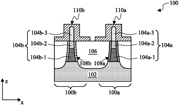
a semiconductor fin over the silicon substrate;
an isolation structure over the silicon substrate, wherein the semiconductor fin includes a first portion and a second portion over the first portion and a third portion under the first portion, the first portion and the third portion are surrounded by the isolation structure, the second portion protrudes above the isolation structure, the second portion has a different crystalline lattice constant than the first portion, the first portion includes a first dopant, and the second portion is substantially free of the first dopant;
a doped material layer between the isolation structure and the first portion of the semiconductor fin, wherein the doped material layer is disposed above the third portion of the semiconductor fin; and
a gate structure above the isolation structure and engaging multiple surfaces of the second portion.
|