| CPC H01L 27/0886 (2013.01) [H01L 21/02205 (2013.01); H01L 21/02211 (2013.01); H01L 21/28088 (2013.01); H01L 21/28556 (2013.01); H01L 21/76224 (2013.01); H01L 21/823431 (2013.01); H01L 21/823437 (2013.01); H01L 21/823462 (2013.01); H01L 21/823481 (2013.01); H01L 29/0649 (2013.01); H01L 29/42372 (2013.01); H01L 29/4966 (2013.01); H01L 29/513 (2013.01); H01L 29/66545 (2013.01); H01L 21/0262 (2013.01); H01L 21/02532 (2013.01); H01L 21/02579 (2013.01); H01L 21/31053 (2013.01); H01L 29/517 (2013.01); H01L 29/7848 (2013.01)] | 13 Claims |
|
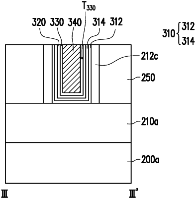
1. A gate structure, comprising:
a gate dielectric layer;
a work function layer surrounded by the gate dielectric layer;
a metal layer disposed over the work function layer; and
a barrier layer surrounded by the work function layer, wherein the barrier layer surrounds the metal layer, the barrier layer comprises fluorine and silicon, or fluorine and aluminum, and the barrier layer is a tri-layered structure.
|