| CPC H01L 27/0886 (2013.01) [H01L 21/0337 (2013.01); H01L 21/823418 (2013.01); H01L 21/823431 (2013.01); H01L 21/823437 (2013.01); H01L 21/823468 (2013.01); H01L 29/0649 (2013.01); H01L 29/66545 (2013.01); H01L 29/785 (2013.01)] | 20 Claims |
|
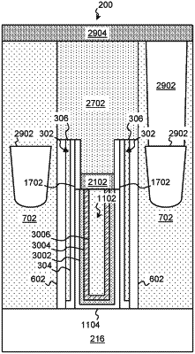
1. A device comprising:
a fin structure disposed on a substrate;
a first gate stack disposed on the fin, the first gate stack including a gate dielectric layer;
a first inner sidewall spacer disposed on the first gate stack, the first inner sidewall spacer having a bottom surface facing the substrate and wherein the bottom surface of the first inner sidewall spacer interfaces with the gate dielectric layer;
a first outer sidewall spacer disposed on the first inner sidewall spacer;
a second inner sidewall spacer disposed on the first gate stack, the second inner sidewall spacer being spaced apart from the first inner sidewall spacer; and
a dielectric capping layer including a first portion disposed between the first and second inner sidewall spacers and a second portion disposed over the first and second inner sidewall spacers, the second portion of the dielectric capping layer being wider than the first portion of the dielectric capping layer.
|