| CPC H01L 27/0716 (2013.01) [H01L 29/0615 (2013.01); H01L 29/0657 (2013.01); H01L 29/0847 (2013.01); H01L 29/1095 (2013.01); H01L 29/32 (2013.01); H01L 29/41708 (2013.01); H01L 29/4236 (2013.01); H01L 29/7397 (2013.01); H01L 29/8611 (2013.01); H01L 29/8613 (2013.01); H01L 29/407 (2013.01)] | 15 Claims |

|
1. A semiconductor device comprising a semiconductor substrate, comprising
an upper-surface electrode provided on an upper surface of the semiconductor substrate;
a lower-surface electrode provided on a lower surface of the semiconductor substrate;
a transistor portion provided in the semiconductor substrate and connected to the upper-surface electrode and the lower-surface electrode;
one or more first diode portions provided in the semiconductor substrate connected to the upper-surface electrode and the lower-surface electrode and extending from the upper-surface electrode to the lower-surface electrode;
one or more second diode portions provided in the semiconductor substrate connected to the upper-surface electrode and the lower-surface electrode and extending without a transistor therebetween from the upper-surface electrode to the lower-surface electrode; and
a drift region of a first conductivity type provided inside the semiconductor substrate and spanning throughout the transistor portion, the one or more first diode portions, and the one or more second diode portions,
wherein a resistivity of the one or more first diode portions in a depth direction of the semiconductor substrate is different from a resistivity of the one or more second diode portions in the depth direction of the semiconductor substrate,
wherein the one or more first diode portions and the one or more second diode portions each include (i) an anode region of a second conductivity type provided between the drift region and the upper surface of the semiconductor substrate, and (ii) a cathode region of the first conductivity type provided between the drift region and the lower-surface electrode,
wherein the transistor portion has:
a base region of the second conductivity type provided between the drift region and the upper surface of the semiconductor substrate;
a source region of the first conductivity type provided between the base region and the upper surface of the semiconductor substrate, the source region having a higher doping concentration than the drift region; and
a gate trench portion provided from the upper surface of the semiconductor substrate so as to reach the drift region, the gate trench portion being provided to extend along a predetermined extending direction on the upper surface of the semiconductor substrate;
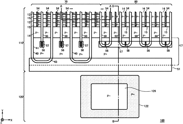
wherein a first well region is provided to overlap, on the upper surface of the semiconductor substrate, an edge part of the gate trench portion in an extending direction, and provided from the upper surface of the semiconductor substrate to a position deeper than the edge part of the gate trench portion, the first well region having a higher doping concentration than the base region;
wherein a second well region is provided adjacent the first well region on the upper surface of the semiconductor substrate separating the one or more first diode portions and the transistor portion from the one or more second diode portions by surrounding and directly contacting along the entirety of the periphery thereof the anode region of the one or more second diode portions;
wherein a distance separates the first well region and the second well region;
wherein the cathode region is in direct contact with the lower-surface electrode.
|