| CPC H01L 25/167 (2013.01) [G06F 3/044 (2013.01); G06F 3/0412 (2013.01); G06F 3/0416 (2013.01); H01L 24/24 (2013.01); H01L 24/25 (2013.01); H01L 33/60 (2013.01); G06F 2203/04105 (2013.01); H01L 33/32 (2013.01); H01L 2224/245 (2013.01); H01L 2224/24051 (2013.01); H01L 2224/24147 (2013.01); H01L 2224/2512 (2013.01); H01L 2224/25175 (2013.01); H01L 2924/0549 (2013.01); H01L 2924/12041 (2013.01); H01L 2924/12043 (2013.01)] | 24 Claims |
|
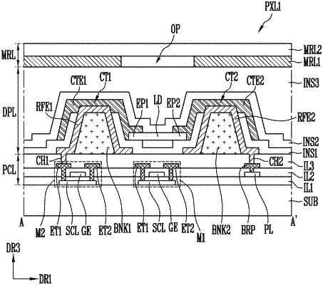
1. A display device comprising:
a substrate;
a first electrode and a second electrode on the substrate;
a light emitting element electrically connected to the first electrode and the second electrode;
a first reflective layer on the light emitting element and including an opening overlapping the light emitting element;
a first insulation layer that at least partially covers the first electrode and the second electrode and is located between the light emitting element and the substrate;
a third electrode on the first electrode and being in contact with one end portion of the light emitting element;
a fourth electrode on the second electrode and being in contact with the other end portion of the light emitting element; and
a second insulation layer that covers the light emitting element, the third electrode, and the fourth electrode,
wherein the first reflective layer comprises a material having a first reflectivity,
wherein the first insulation layer includes a first area and a second area, and
wherein the third electrode contacts the first electrode through the first area, and the fourth electrode contacts the second electrode through the second area.
|