| CPC H01L 25/167 (2013.01) [H01L 27/124 (2013.01); H01L 27/1248 (2013.01); H01L 27/1259 (2013.01); H01L 33/60 (2013.01)] | 20 Claims |
|
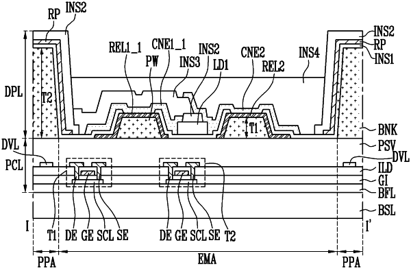
1. A display device comprising:
a base layer including a display area and a non-display area; and
a plurality of pixels disposed in the display area, each of the plurality of pixels including a plurality of sub-pixels, wherein
each of the plurality of sub-pixels comprises:
a pixel circuit layer; and
a display element layer disposed on the pixel circuit layer,
each display element layer comprises:
a partition wall disposed in each of the plurality of sub-pixels;
a bank disposed between adjacent ones of the plurality of sub-pixels, the bank having a greater thickness than the partition wall;
a first electrode and a second electrode disposed on the partition wall and spaced apart from each other;
a reflective pattern disposed on the bank; and
at least one light emitting element disposed between the first electrode and the second electrode wherein
the reflective pattern encloses an upper surface and a side surface of the bank.
|