| CPC H01L 25/0657 (2013.01) [H01L 21/561 (2013.01); H01L 21/78 (2013.01); H01L 23/3128 (2013.01); H01L 23/49822 (2013.01); H01L 23/49827 (2013.01); H01L 23/552 (2013.01); H01L 23/562 (2013.01); H01L 23/60 (2013.01); H01L 25/105 (2013.01); H01L 25/50 (2013.01); H01L 21/486 (2013.01); H01L 21/568 (2013.01); H01L 23/49805 (2013.01); H01L 23/5389 (2013.01); H01L 2224/18 (2013.01); H01L 2224/32145 (2013.01); H01L 2224/48091 (2013.01); H01L 2224/48227 (2013.01); H01L 2224/73265 (2013.01); H01L 2225/0651 (2013.01); H01L 2225/06548 (2013.01); H01L 2225/06568 (2013.01); H01L 2924/181 (2013.01)] | 20 Claims |
|
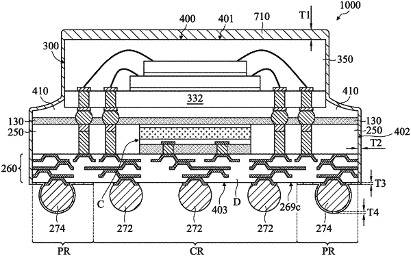
1. A chip package structure, comprising:
a chip structure;
a first ground bump below the chip structure; and
a conductive shielding film disposed over the chip structure and extending onto the first ground bump, wherein the conductive shielding film has a curved bottom surface.
|