| CPC H01L 25/0657 (2013.01) [H01L 23/3107 (2013.01); H01L 23/481 (2013.01); H01L 2225/06517 (2013.01)] | 20 Claims |
|
1. A semiconductor package, comprising:
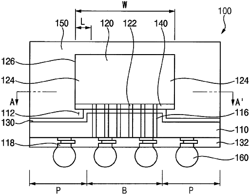
a first semiconductor chip including a plurality of connection vias and a wiring connected to lower ends of the plurality of connection vias;
a second semiconductor chip disposed on a central portion of an upper surface of the first semiconductor chip, the second semiconductor chip including bonding pads configured to directly contact upper ends of the plurality of connection vias; and
a molding member formed on the upper surface of the first semiconductor chip, the molding member at least partially surrounding the second semiconductor chip,
wherein the plurality of connection vias are disposed on the central portion of the upper surface of the first semiconductor chip, and the central portion of the upper surface of the first semiconductor chip is at a higher level than an edge portion of the upper surface of the first semiconductor chip, relative to a package substrate, and
wherein an edge portion of the second semiconductor chip is horizontally protruded from the central portion of the upper surface of the first semiconductor chip to form an overhang that is spaced apart from the edge portion of the upper surface of the first semiconductor chip, the overhang having a horizontal length of about 3/20 times to about 9/20 times a width of the second semiconductor chip, and a distance between a lower surface of the overhang and the edge portion of the upper surface of the first semiconductor chip is no less than about 8 μm.
|