| CPC H01L 24/83 (2013.01) [H01L 21/265 (2013.01); H01L 21/6835 (2013.01); H01L 21/7806 (2013.01); H01L 25/50 (2013.01)] | 20 Claims |
|
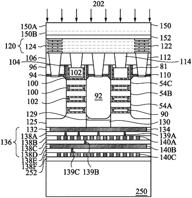
1. A method comprising:
forming a transistor structure of a device on a first semiconductor substrate;
forming a front-side interconnect structure over a front side of the transistor structure;
bonding a carrier substrate to the front-side interconnect structure;
after bonding the carrier substrate to the front-side interconnect structure, implanting ions into the first semiconductor substrate to form an implantation region of the first semiconductor substrate;
removing the first semiconductor substrate, wherein removing the first semiconductor substrate comprises:
applying an annealing process to separate the implantation region from a remainder region of the first semiconductor substrate; and
forming a back-side interconnect structure over a back side of the transistor structure.
|