| CPC H01L 24/25 (2013.01) [H01L 21/4853 (2013.01); H01L 21/568 (2013.01); H01L 23/49816 (2013.01); H01L 23/5389 (2013.01); H01L 24/13 (2013.01); H01L 24/24 (2013.01); H01L 24/73 (2013.01); H01L 24/82 (2013.01); H01L 24/92 (2013.01); H01L 2224/13022 (2013.01); H01L 2224/24137 (2013.01); H01L 2224/24227 (2013.01); H01L 2224/2501 (2013.01); H01L 2224/25171 (2013.01); H01L 2224/73209 (2013.01); H01L 2224/73267 (2013.01); H01L 2224/821 (2013.01); H01L 2224/82005 (2013.01); H01L 2224/92244 (2013.01)] | 20 Claims |

|
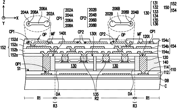
1. A package structure, comprising:
a semiconductor die having an active side, comprising a plurality of conductive vias disposed on the active side and a dielectric layer disposed over the active side and covering a sidewall of the plurality of conductive vias;
an insulating encapsulation, encapsulating the semiconductor die, wherein the active side and the plurality of conductive vias of the semiconductor die are separated from the insulating encapsulation through the dielectric layer;
a first redistribution circuit structure, disposed on a first side of the insulating encapsulation and electrically coupled to the semiconductor die; and
a second redistribution circuit structure, disposed on a second side of the insulating encapsulation and electrically coupled to the semiconductor die, the second side being opposite to the first side.
|