| CPC H01L 24/09 (2013.01) [H01L 24/25 (2013.01); H01L 24/73 (2013.01); H01L 24/81 (2013.01); H01L 2224/09181 (2013.01); H01L 2224/2541 (2013.01); H01L 2224/73209 (2013.01); H01L 2224/81801 (2013.01)] | 22 Claims |
|
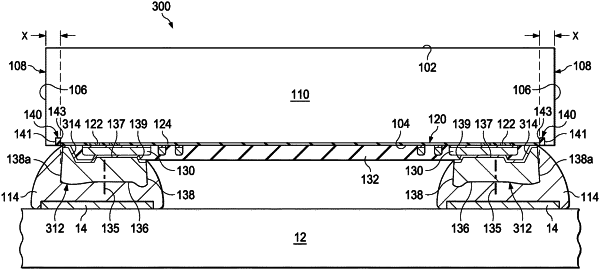
1. A wafer chip scale package (WCSP), comprising:
a semiconductor die having a device side in which a circuit is formed;
a redistribution layer (RDL) coupled to the device side that is positioned within an insulating member;
a scribe seal circumscribing the circuit along the device side, wherein the RDL abuts the scribe seal; and
a conductive member coupled to the RDL, wherein the conductive member is configured to receive a solder member, and wherein the insulating member is absent on the device side of the semiconductor die between the conductive member and a portion of an outer perimeter of the WCSP closest to the conductive member.
|