| CPC H01L 24/06 (2013.01) [H01L 21/4814 (2013.01); H01L 21/4846 (2013.01); H01L 21/4853 (2013.01); H01L 23/49816 (2013.01); H01L 23/5223 (2013.01); H01L 24/02 (2013.01); H01L 24/05 (2013.01); H01L 24/07 (2013.01); H01L 24/10 (2013.01); H01L 24/13 (2013.01); H01L 24/16 (2013.01); H01L 2224/0401 (2013.01); H01L 2224/05005 (2013.01); H01L 2224/05008 (2013.01); H01L 2224/05015 (2013.01); H01L 2224/05555 (2013.01); H01L 2224/0603 (2013.01); H01L 2224/16227 (2013.01)] | 20 Claims |

|
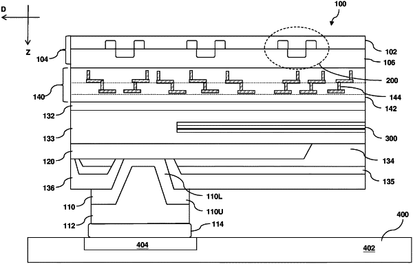
10. A device package, comprising:
a rectangular substrate having four corners and four triangular regions, each of the four triangular regions sharing one of the four corners with the rectangular substrate, the four triangular regions defining a first region and an area of the rectangular substrate outside the first region defining a second region;
a plurality of first-type contact pads disposed directly over the first region;
a plurality of second-type contact pads disposed directly over the second region; and
a plurality of under-bump metallization (UBM) features, each of the plurality of UBM features being disposed directly over one of the plurality of first-type contact pads,
wherein each of the plurality of first-type contact pads is different from each of the plurality of second-type contact pads,
wherein a vertical projection area of each of the plurality of UBM features falls completely within a vertical projection area of the underlying one of the plurality of first-type contact pads.
|