| CPC H01L 23/66 (2013.01) [H01L 24/20 (2013.01); H01L 2223/6616 (2013.01); H01L 2223/6677 (2013.01); H01L 2924/1421 (2013.01)] | 16 Claims |
|
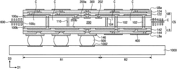
1. A semiconductor device, comprising:
a substrate, a bottom surface of the substrate including first and second regions spaced apart from each other;
a first semiconductor chip buried in the substrate, the first semiconductor chip having a first active surface that is directed to a top surface of a core portion of the substrate;
a first antenna pattern provided on the top surface of the substrate and electrically connected to the first semiconductor chip;
a second antenna pattern provided on the first region of the bottom surface of the substrate; and
outer terminals provided on the second region of the bottom surface of the substrate,
wherein the first antenna pattern is connected to first chip pads, which are provided on the first active surface of the first semiconductor chip, through an upper buildup portion of the substrate,
wherein the second antenna pattern is connected to the first chip pads of the first semiconductor chip through a vertical connection terminal, which extends from a bottom surface of the upper buildup portion of the substrate to a top surface of a lower buildup portion of the substrate, and
wherein the first active surface of the first semiconductor chip is in contact with the upper buildup portion.
|