| CPC H01L 23/544 (2013.01) [H01L 23/145 (2013.01); H01L 23/32 (2013.01); H01L 25/0655 (2013.01)] | 20 Claims |
|
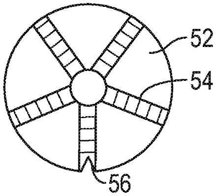
1. A semiconductor substrate comprising:
a uniformly thinned wafer comprising a first side and a second side; and
a support structure separate from a material of the uniformly thinned wafer coupled to the uniformly thinned wafer at a desired location on the first side, the second side, or both the first side and the second side;
wherein the support structure comprises an organic compound;
wherein the support structure comprises a first spoke, a second spoke, and a third spoke; and
wherein an area of the support structure is smaller than an area of either the first side or the second side.
|