| CPC H01L 23/5389 (2013.01) [H01L 21/4853 (2013.01); H01L 21/4857 (2013.01); H01L 21/565 (2013.01); H01L 21/568 (2013.01); H01L 21/6835 (2013.01); H01L 23/3128 (2013.01); H01L 23/5383 (2013.01); H01L 23/5386 (2013.01); H01L 24/19 (2013.01); H01L 24/20 (2013.01); H01L 25/0657 (2013.01); H01L 25/105 (2013.01); H01L 2221/68372 (2013.01); H01L 2224/214 (2013.01); H01L 2225/0651 (2013.01); H01L 2225/06568 (2013.01); H01L 2225/06586 (2013.01); H01L 2225/1035 (2013.01); H01L 2225/1058 (2013.01)] | 20 Claims |
|
1. A method comprising:
attaching a die to a carrier substrate, the die comprising a first connector, a second connector, and a third connector;
forming an encapsulant over the carrier substrate and along sidewalls of the die; and
forming a redistribution structure over the die and the encapsulant, wherein forming the redistribution structure comprises:
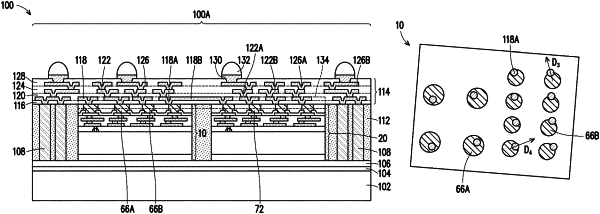
forming a first redistribution layer, a first via of the first redistribution layer being in physical contact with the first connector, the first via being laterally offset from the first connector by a first non-zero distance in a first direction, the first via having a tapered sidewall, a second via of the first redistribution layer being in physical contact with the second connector, the second via being laterally offset from the second connector by a second non-zero distance in a second direction, the second via having a tapered sidewall, a third via of the first redistribution layer being in physical contact with the third connector, the third via being laterally offset from the second connector by a third non-zero distance in a third direction, the third via having a tapered sidewall, wherein the first direction is different from the second direction and the third direction, wherein the second direction is different from the third direction.
|
|
9. A method of forming a semiconductor device, the method comprising:
encapsulating a die in an encapsulant, the die comprising a first connector, a second connector, a third connector, and a fourth connector;
forming a redistribution structure over the die and the encapsulant, wherein forming the redistribution structure comprises:
forming a first via in physical contact with the first connector, the first via being laterally offset from the first connector by a first non-zero distance in a first direction, the first via having a tapered sidewall;
forming a second via in physical contact with the second connector, the second via being laterally offset from the second connector by a second non-zero distance in a second direction different from the first direction;
forming a third via in physical contact with the third connector, the third via being laterally offset from the third connector by a third non-zero distance in a third direction different from the first direction and the second direction; and
forming a fourth via in physical contact with the fourth connector, the fourth via fully landing on the fourth connector.
|
|
16. A method of forming semiconductor device, the method comprising:
forming an encapsulant along sidewalls of a first die and a second die, the first die comprising a first connector and a second connector, the second die comprising a third connector and a fourth connector; and
forming a redistribution structure over the first die and the second die, wherein a first via of the redistribution structure is in physical contact with a top surface of the first connector, wherein the first connector fully overlaps with the first via in a plan view, wherein a second via of the redistribution structure is in physical contact with a top surface of the second connector, wherein the second connector partially overlaps the second via in the plan view, the second via being laterally offset from the second connector by a first non-zero distance in a first direction, wherein a third via of the redistribution structure is in physical contact with a top surface of the third connector, wherein the third connector partially overlaps the third via in the plan view, the third via being laterally offset from the third connector by a second non-zero distance in a second direction different from the first direction, and wherein a fourth via of the redistribution structure is in physical contact with a top surface of the fourth connector, wherein the fourth connector partially overlaps the fourth via in the plan view, the fourth via being laterally offset from the fourth connector by a third non-zero distance in a third direction different from the first direction and the second direction.
|