| CPC H01L 23/535 (2013.01) [H10B 43/40 (2023.02)] | 20 Claims |
|
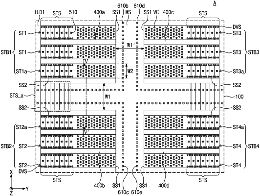
1. A three-dimensional (3D) semiconductor memory device comprising:
a peripheral circuit structure comprising peripheral transistors formed with a substrate;
a semiconductor layer on the peripheral circuit structure;
first to fourth blocks on the semiconductor layer, each of the first to fourth blocks including a plurality of gate electrodes vertically stacked on the semiconductor layer; and
a separation structure disposed on the semiconductor layer, the separation structure including a first portion extending a first direction and a second portion crossing the first portion and extending a second direction intersecting the first direction,
wherein the first portion of the separation structure is disposed between the first and second blocks and between the third and fourth blocks, and
wherein the second portion of the separation structure is disposed between the first and third blocks and between the second and fourth blocks.
|