| CPC H01L 23/5329 (2013.01) [H01L 21/7682 (2013.01); H01L 23/5226 (2013.01); H10B 63/84 (2023.02); H01L 21/764 (2013.01); H10B 43/30 (2023.02); H10B 63/24 (2023.02); H10N 70/231 (2023.02); H10N 70/24 (2023.02); H10N 70/826 (2023.02); H10N 70/8413 (2023.02)] | 8 Claims |
|
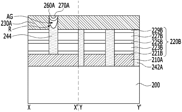
1. A method for fabricating an electronic device comprising a semiconductor memory, the method comprising:
forming a first conductive layer and a memory material over a substrate;
etching the first conductive layer and the memory material layer using a first mask pattern having a line shape extending in a first direction to form lower lines and memory material patterns extending in the first direction;
forming a second conductive layer over the memory material patterns;
etching the second conductive layer and the memory material patterns using a second mask pattern having a line shape extending in a second direction crossing the first direction to form upper lines extending in the second direction and pillar shaped memory cells;
forming an insulating layer between the memory cells and the upper lines; and
forming an air gap within the insulating layer, the air gap being located between the upper lines and extending in the second direction.
|